|
|
|
|
& |
|
In this project, we present an implementation example for the PLX1.0 ISA developed in Princeton University. We describe a 2-way superscalar implementation of the PLX Processor, using VHDL as the design entry tool. This implementation may support all instructions described in the PLX1.0 specification and was verified at logic level via VHDL simulators such as SYNOPSYS. Our design methodology is a combination of structural and behavioral modeling: all blocks that is driven by clocks, such as all registers, are designed at structural level. This is to ensure that the whole processor works like a "real" hardware implementation and once it is verified, the clock timing of the processor is verified. While for complicated combinational logic, we use behavioral description since combinational logic will not cause timing problems if we don't make the critical path too long. This approach brings us more flexibilities and makes debugging easier. Further more, it's not a difficult work to convert a behavioral description of a combinational logic into a synthesizable description and thus one can easily make the whole design synthesizable when necessary. The top level block diagram of our design is shown in figure I-6. The lower hierarchy block descriptions are imported from other group modules, which are done in RTL level. Both the test vectors (binaries+clock+initialization signals) and assembly level codes are included in this documentation. In order to provide flexibility in testing of top level design, an assembler is also written in VHDL to acquire the binary instruction sequence. The structural design is expatiated with block diagram descriptions, the verification of operation is demonstrated using waveform diagrams and simulation outputs.
| 0) TABLE OF CONTENTS: |
0)Table of Contents
1) Introduction
2) Design
and Implementation
3) Simulation
Results
4) Appendices
| 1) INTRODUCTION: |
PLX is a small, general purpose, subword parallel ISA, implemented in
Princeton University by Prof. Lee and Princeton students. The major objective
of PLX is toward multimedia applications and specifically 3GPP applications
and protocols. The PLX Project Part-II comprises of 3 major subdivisions,
depending on the nature of the project work, Algorithms, Software and Hardware.
Our project Hardware- is VHDL design of a 2-way pipelined superscalar
implementation of the PLX-Processor, with the hazard detection and bypassing
logic. Being a principal feature of PLX ISA, predication which is used
in PLX and IA64 instead of conditional branches is also implemented in
the hardware control logic. As the case in most cost effective implementation,
although the execution units are doubled for superscalarity, there is a
single Data Cache in the datapath. Regarding the general pipeline control
path, the control signals are also piped through the pipe stages. The major
execution units, ALU, Shift-Permute Unit and Multiplier are designed incompletely
in behavioral level and are to be provided by other hardware groups working
on the lower hierarchy RTL design. In addition to the hardware description
of the data and control paths, we also implemented an assembler in VHDL
to convert the assembly level instructions to binary instructions. The
assembler is integrated with the final testbench, to provide both the resultant
binary file and instruction information for the processor. The design of
the assembler allows us a higher flexibility for application of different
test programs.
| 2) DESIGN and IMPLEMENTATION: |
In this section, we describe the design of the 2-way superscalar PLX processor in detail, and as clearly as possible. We follow a design top-down and implement bottom-up procedure, yet the description will be from lower hierarchy cells to higher level design. The discussion of the assembler is done after the description of the top-level circuit for the sake of design description flow. However, the implementation of the assembler is actually in parallel with the implementation of the top level design.
In order to explain our design in a clear and logical way, we divide this part into 4 subsections:
Appendix-I lists brief descriptions and some testbenches for the following components.1. ALU2. Multiplier
3. Shift - Permute Unit
4. Predicate Register File
5. General Purpose Register File
6. Instruction Decoder
7. Pipeline Registers
8. Controller
9. Instruction Memory
10. Data Cache
11. Top Level Design
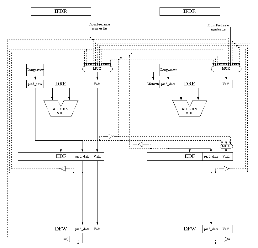
Figure 1 shows the datapath diagram of our 2-way superscalar PLX processor. The data forwarding paths for predicate bits are shown in Figure 2.
- There are two symmetrical pipelines. Each of them has 1 ALU, 1 Shifter and 1 Multiplier. They share one data cache and one load/store pipe. Since both pipe is allowed to use load/store pipe, a data merging structure is necessary. In order to avoid a too long critical path in DF stage (since data cache is the slowest component in the processor), the merging work is done in E stage.
- Standard data forwarding logic for general purpose register file is implemented. One special forwarding path, the WtoE is added to the standard forwarding logic. This path bypasses the data that is being written back to the output of the read port, i.e., the write and read can be performed simultaneously and the original two-phase write/read cycle is not necessary. By introducing this forwarding path, the critical path of DR stage is considerably shortened.
- Since the results of CMP instructions are generated by ALU, i.e., no decisions are available until E stage, its necessary to design and implement data forwarding logic for predicate register file to reduce stalls, especially for complicate logic expression calculation and branch.
- To support PMUL instructions which have a 3-cycle E stage, some special registers, MUL PIPEs, are added to the datapath. These registers help to write results of PMULs back correctly.
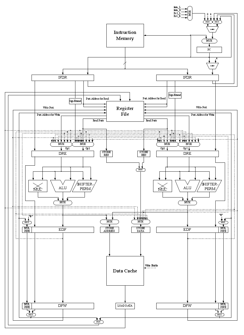
Figure-1, Datapath Diagram of a 2-way superscalar PLX processor
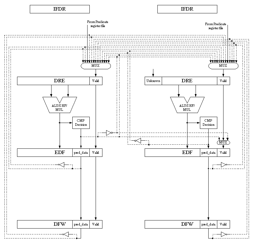
(a) Use ALU to calculate the results of CMP instructions
(b) Use specific comparators to calculate the results of CMP instructions
Figure-2, Data forwarding paths for predicate bits
1. Hazard detection
2. Data forwarding logic for general purpose register file
3. Data forwarding logic for predicate register fileIF/DR0---IF/DR1
Number IF/DR0 IF/DR1 Results 1 ALU/PMUL/LDi/LD/ST.upd ALU/LD/ST/JMP.reg/CMP/PMUL Stall IF/DR1 2 LD/ST LD/ST Stall IF/DR1 3 CMP/CHPR JMP/CHPR Stall IF/DR1 4 CHPR any Stall IF/DR1 DR/E0---IF/DR0
Number DR/E0 IF/DR0 Results 5 PMUL/LD ALU/LD/ST/JMP.reg/CMP/PMUL Stall IF/DR 6 CMP/CHPR CHPR Stall IF/DR DR/E0---IF/DR1
Number DR/E0 IF/DR1 Results 7 PMUL/LD ALU/LD/ST/JMP.reg/CMP/PMUL Stall IF/DR1 8 CMP/CHPR CHPR Stall IF/DR1 DR/E1---IF/DR0
Number DR/E1 IF/DR0 Results 9 PMUL/LD ALU/LD/ST/JMP.reg/CMP/PMUL Stall IF/DR 10 CMP/CHPR CHPR Stall IF/DR Note: For DR/E1, one may not determine whether it is valid or not only from the valid bit read from predicate register since CMP results of DR/E0 may influence DR/E1. Thus before stall IF/DR, the check of validity is necessary.
DR/E0---IF/DR1
Number DR/E0 IF/DR1 Results 11 PMUL/LD ALU/LD/ST/JMP.reg/CMP/PMUL Stall IF/DR1 12 CMP/CHPR CHPR Stall IF/DR1 Note: For DR/E1, one may not determine whether it is valid or not only from the valid bit read from predicate register since CMP results of DR/E0 may influence DR/E1. Thus before stall IF/DR, the check of validity is necessary.
E/DF0---IF/DR0
Number E/DF0 IF/DR0 Results 13 PMUL ALU/LD/ST/JMP.reg/CMP/PMUL Stall IF/DR 14 PMUL any instruction that will write RF except PMUL insructions Stall IF/DR E/DF0---IF/DR1
Number E/DF0 IF/DR1 Results 15 PMUL ALU/LD/ST/JMP.reg/CMP/PMUL Stall IF/DR1 E/DF1---IF/DR0
Number E/DF1 IF/DR0 Results 16 PMUL ALU/LD/ST/JMP.reg/CMP/PMUL Stall IF/DR E/DF1---IF/DR1
Number E/DF1 IF/DR1 Results 17 PMUL ALU/LD/ST/JMP.reg/CMP/PMUL Stall IF/DR 18 PMUL any instruction that will write RF except PMUL insructions Stall IF/DR For JMP instructions:
IF/DR0---IF/DR1
Number IF/DR0 IF/DR1 Results 1 JMP any Cancel IF/DR1(only if JMP is valid and taken) DR/E0&1---IF/DR0&1
Number DR/E0&1 IF/DR0&1 Results 2 JMP any Cancel IF/DR(only if JMP is valid and taken) Note: Thus it's actually a predict-untaken JMP implementation.
All data forwarding paths are shown in figure 1. Table 1 lists the correct data sources of MUXs of Op1 and Op2 for different instructions. Note that the JMP target address is not calculated by ALU. We use a specific adder to calculate it in DR stage.
Instruction MUX for Op1 MUX for Op2 JMP any any JMP.link PC immediate number: 4 JMP.reg any any JMP.reg.link PC immediate number: 4 Loadi.hi/lo any IR_imm trap any any CMP Rs1(or from forwarded data) Rs2(or from forwarded data) CMPi Rs1(or from forwarded data) IR_imm Testbit Rs1(or from forwarded data) IR_imm Changepr any any Changepr.load any any Load Rs1(or from forwarded data) IR_imm Load.upd Rs1(or from forwarded data) IR_imm Store Rs1(or from forwarded data) IR_imm Store.upd Rs1(or from forwarded data) IR_imm ALU/LOGIC imm Rs1(or from forwarded data) IR_imm Extract Rs1(or from forwarded data) IR_imm Deposit Rs1(or from forwarded data) IR-imm Shift Right Pair Rs1(or from forwarded data) Rs2(or from forwarded data) Packed ALU/SHIFT_PERM Rs1(or from forwarded data) Rs2(or from forwarded data) Packed MUL Rs1(or from forwarded data) Rs2(or from forwarded data) Packed SHIFT_PERM with imm Rs1(or from forwarded data) IR_imm Table-1, Data Sources for MUXs of Op1&Op2
For Rsi(or from forwarded data), once the target/source addresses are the same and the source instruction is valid, the data should be forwarded.
According to figure 2, the results of CMP instructions are not available until E stage. But with the data forwarding logic, the validity of all instructions can be determined in DR stage except one case: when CMP in IFDR0, then the validity of the instruction in IFDR1 can be determined in E stage. Thus only the instructions that complete the "real" operations in DR stage, such as JMP and Changepr, have to be stalled in this case.When Changepr in IFDR0, any instruction in IFDR1 has to be stalled since Changepr modified the bank selection bits of the predicate register file in DR stage, thus one can not know whether the instruction is valid. Figure 3 shows the circuit of bank selection bits.
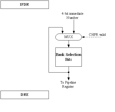
Figure-3, Bank selection unit
1. Assembler
2. Final Testbench
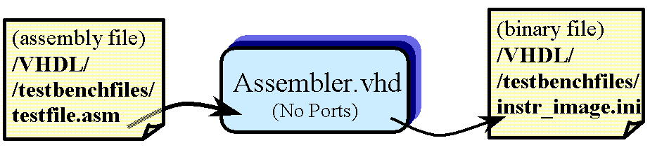
In order to avoid directly manipulating binary streams for instructions, we implemented an assembler in VHDL, as shown in assembler.vhd, which is integrated with the testbench to read instructions directly from an assembly file and convert the assembly level instructions to binary instructions stored in the instruction memory. The assembler is written as flexibly as possible, providing flexible file formats as well as several informative error diagnostics. The input output of the assembler is as shown in figure-4.
In order to demonstrate the flexibility of the assembler, we provide an exemplary testfile.asm and demonstrate the cases on this file:
| #OUR ASSEMBLY FILE:
P7:cmp.leu R1, R11, P1,P0
p0: PADD.8.u r5 , r3, r2 #comment here P2:jmp.link -1 # MY ASSEMBLY CODE NEEDS THIS , 0
# wrong instructions
|
|
Hence, we also demonstrated a bug-like property of the program for jmp.reg instruction, yet this is not a bug as done intentionally to make jmp.reg abide by Type-1 instructions, and can be fixed if needed.The assembler has several error diagnostic properties to help determine and correct the faulty instructions and several debug options embedded in the code. At present, some of the debug options are still left working as they are informative in verification of correct operation. The output of the simulator with respect to the above file and the generated binary file are shown in table-2.
|
|
|
| <<<<<<<<<<<<<<<<<<<
STARTS >>>>>>>>>>>>>>>>>>
11100100000001010110000010000111 11000010000110111111111111110111 00011000000011000100010100000111 01000000111111111111111111111111 00000001010010000000000000000000 0 NS Assertion FAILURE at 0 NS in design unit ASSEMBLER(TESTBENCH) from process /ASSEMBLER/_P0: "test finished" |
binary instruction also on standard output
|
|
|
|
| 11100100000001010110000010000111
11000010000110111111111111110111 00011000000011000100010100000111 01000000111111111111111111111111 00000001010010000000000000000000 |
In order to demonstrate the diagnostic ability of our assembler, we include a few exemplary cases of error reports, as shown in table 3. The assembler error diagnostics include,but are not limited to the given examples.
|
|
|
| PADD.8.u r5 , r3, r2 #comment here | ***ERROR***: in line -> 6
"Invalid instruction[non numeric Predicate id] -->PADD.8.u r5 , r3, r2 #comment here " |
| P7:cmp.leu R1, R11 P1,P0 | "Invalid instruction -->P7:cmp.leu R1, R11 P1,P0" |
| P3:padd.5.u r5, r4, r3 | ***ERROR***: in line -> 7
"Invalid instruction [wrong subword size field for ...] -->padd.5.u r5, r4, r3" |
| P8:psub.4.s r5, r4, r3 | ***ERROR***: in line -> 7
"Invalid instruction[non numeric Predicate id] -->P8:psub.4.s r5, r4, r3" |
| P4:psub.4. r5, r4, r3 | ***ERROR***: in line -> 11
"Invalid instruction [expected u or s for psub] -->P4:psub.4. r5, r4, r3" |
| P6 : loadi.hi 6, -9 | ***ERROR***: in line -> 5
"Invalid instruction[expected Rd register field] -->P6 : loadi.hi 6, -9" |
This assembler file is seen to be very effective in generating the required binary data for the instruction memory, and is as a matter of fact integrated within the final testbench. As a mean of precaution, the assembler code should be run with:
statement in ".synopsys_vss.setup" simulation setup file, otherwise, the assertion statements do not cause the simulation to terminate. Other determined bugs for the assembler code are, tabs between fields are not sufficient toseparate fields, and immediate value is taken in the range -99999 to 99999 decimal, therefore, all the 23 bit immediates are not supported (Hence, 99999 is up to 17 bits only), but this can be fixed if needed. Finally, although all cases are tried to be taken care of, a space after the end of each instruction is recommended - Although we have not encountered any case this is actually recommended, the final field handled as a special case in the assembler due to possibility of exceeding available line length in comparison of fields, and a space solves this special case.
| 3) SIMULATION RESULTS: |
The following asm files and binary files as shown in tables 4 and 5
are examples of our testbenches: Standard data forwarding, predicate register
control, compare and jump all appear in these testbenches.
3.1) FIBONACCI SEQUENCE:
This test file computes the first 100 terms of the Fibonacci Series.
The assembly level file, fibo.asm
is input to the assembler and the resulting binary file, fibo.bin
is used by the instruction memory to store
the binary instructions.
ASM file |
Binary file |
|
#
PROGRAM TO COMPute FIBONACCI
P1:
LOADI.LO r1, 1
P1:
loadi.lo R2, 32
#
R1 and R2 keep for loop repetition
P1:
loadi.lo r3,1
P1:
loadi.lo R4,0
#
R3 and R4 first 2 terms of fibonacci
P1:padd.8
R5,R3,R0
#R0
contaions 0 and R5 is tmp
P1:
padd.8 R3, R3,R4
P1:
padd.8 R4, R5, R0
P1:
psub.8 R2,R2,R1
P1:
cmp.gt R2, R0, P1, P2
P1:
jmp -20
#
jump back 5 instr-s
P2:
padd.8 R10, R3, R0
#
to see that now P2 is set
|
00100010100001000000000000000001
00100010100010000000000000100000 00100010100011000000000000000001 00100010100100000000000000000000 00111000000011000000010100000011 00111000000011001000001100000011 00111000000101000000010000000011 00111000000010000010001000010011 00100100000010000000000010100100 00100000011111111111111111101100 01011000000011000000101000000011 |
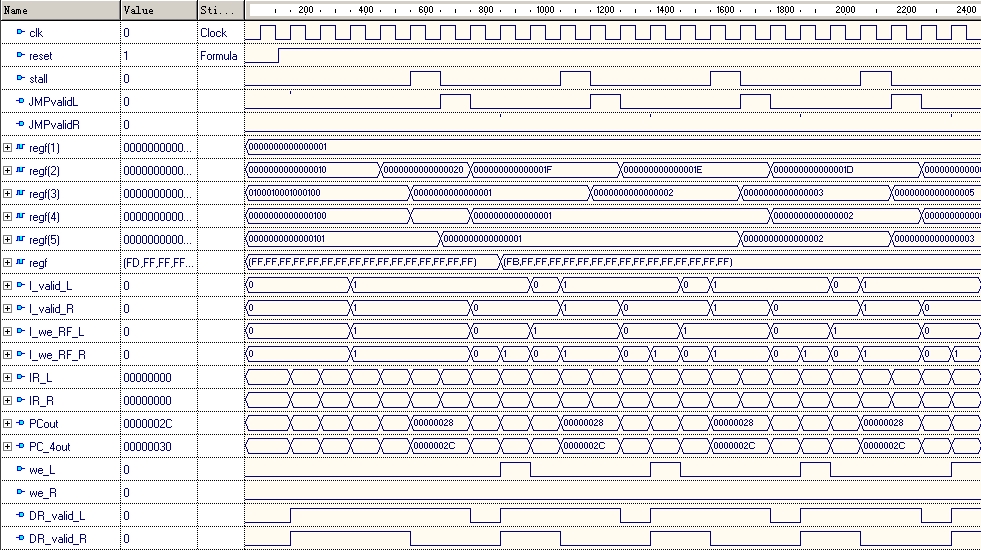
Figure-5, Simulation waveform for fibo.asm
3.2) FAXPY SEQUENCE:
This test file computes the fixed point: a*x[i]+y[i] for arrays x and
y terms of the Fibonacci Series. The assembly level file, faxpy.asm
is the assembly level file and the resulting binary file, faxpy.bin
is used by the instruction memory to store
the binary instructions.
ASM file |
Binary file |
|
#
PROGRAM TO COMPUTE FAXPY
# P0:mux.2.brcst R3, R3 #copy scalar "a" to all 16-bit subwords in R3 #foo: P1:LOAD.8.upd R4, 8(R1) #load (X(i), X(i+1), X(i+2), X(i+3)), update R1 P1:PMUL.odd R5, R4,R3 #multiply (a*X(i), a*X(i+2)) P1:PMUL.even R6, R4,R3 #multiply (a*X(i+1), a*X(i+3)) P1:LOAD.8 R8, 8(R2) #load (Y(i), Y(i+1), Y(i+2), Y(i+3)) P1:MIX.2.L R7, R8,R0 #expand 16-bit to 32-bit subwords, padding on right P1:MIX.2.R R8, R8,R0 #R7=(Y(i), Y(i+2)) and R8=(Y(i+1), Y(i+3)) P1:PADD.4 R9, R5,R7 #add (a*X(i)+Y(i), a*X(i+2)+Y(i+2)) P1:PADD.4 R10, R6,R8 #add (a*X(i+1)+Y(i+1), a*X(i+3)+Y(i+3)) P1:MIX.2.L R8, R9,R10 #contract 32-bit down to 16-bit subwords P1:STORE.8.upd 8(R2), R8 #store new (Y(i), Y(i+1), Y(i+2), Y(i+3)), update R2 P1:CMP.leu R1,R11, P1,P0 #test if done (result to P0 is discarded) P1:JMP -44 #loop if not done |
00101011100001001000000000001000
00111000100100000110010100000001 00111000100100000110011000000101 00101001100010010000000000001000 00111001001000000000011101000001 00111001001000000000100001000101 00111000000101001110100100000010 00111000000110010000101000000010 00111001001001010100100001000001 00101111100010010000000000001000 00100100000001010110000010000111 00100000011111111111111111010100 |
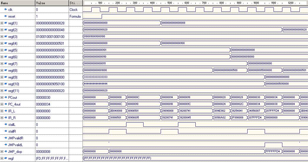
Figure-6, simulated waveform for one loop of FAXPY
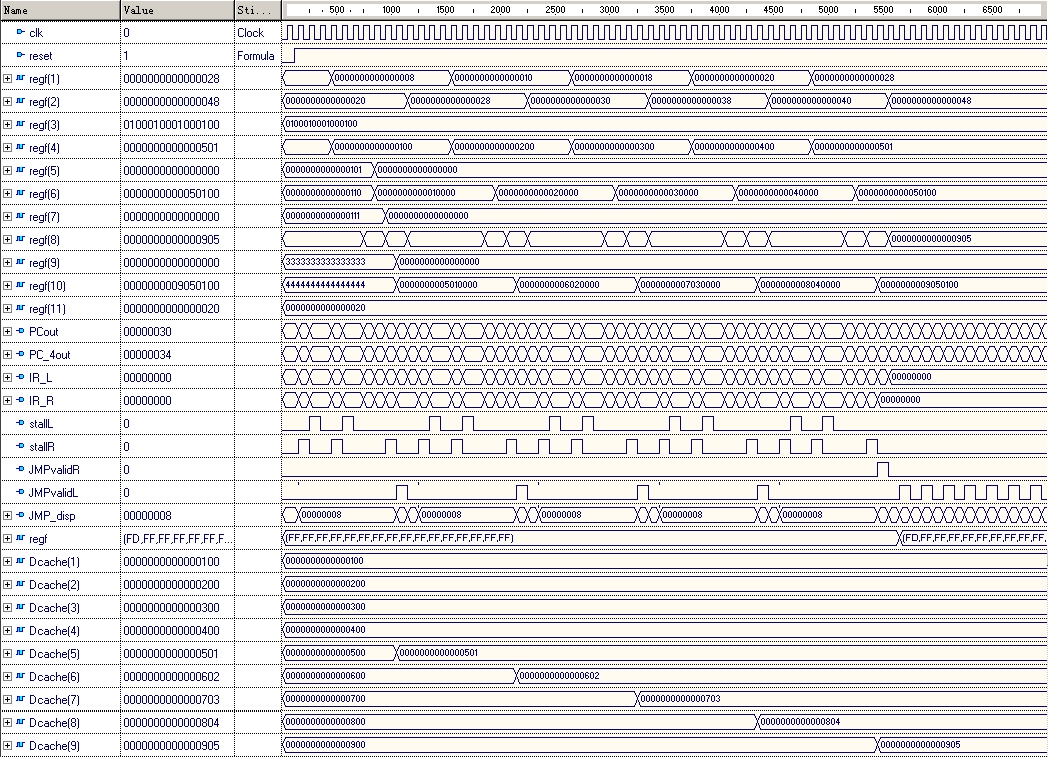
Figure-7, simulated waveform for 5 loops of FAXPY
| 4) APPENDICES |
4.1) APPENDIX-I
- BASIC COMPONENT LIST:
In order to test our processor, we implemented a behavioural level ALU, as included in ALU64_new.vhd. This ALU performs not all, but the required basic functions for our testbenches such as:4.1.2 MULTIPLIER:and is used in most of the testings. A representative block diagram for the ALU, demonstrating the input and output pins is shown in figure I-1.
and the new permute instruction included in the ISA:
- padd.sw
- cmp
- psub.sw
- loadi.hi/lo
- load.8.update
- load.8
- store.8.update
- mux.2.brcst
A representative simulation for the ALU is done using the test program ALU64_tester.vhd within the higher level testbench file. The simulation stimulus, waveforms and descriptions are shown in Appendix-II.
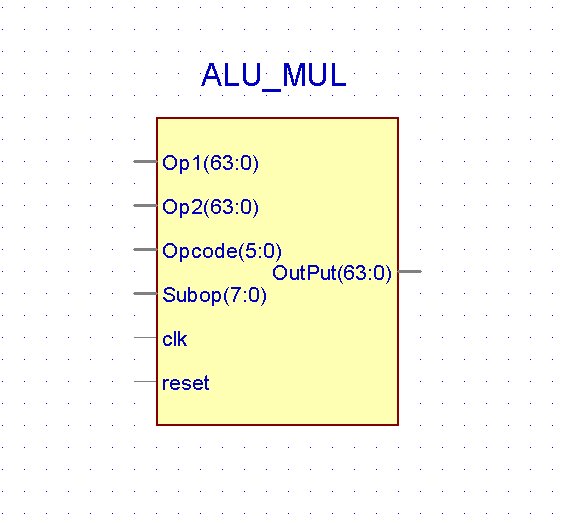
Figure I-1, ALU/Multiplier
To support PMUL instructions, we also implemented a behavior-level fix-point multiplier, as shown in MUL.vhd. In our design, multipliers have a 3-cycle E stage and are pipelined. Up to now, PMUL.odd and PMUL.even are implemented. Its input/output pins are almost the same as ALU except that MUL needs clk and reset inputs.4.1.3 SHIFT-PERMUTE UNIT:
For the shift permute unit, we use the shift permute unit provided by group 1. The behavioral design for the shift permute unit is shown in 1-shift-permute.vhd.
As described in PLX-1.0, we implemented a 16-bank predicate register file, and each bank contains 8 bits, which is shown in pred_reg_v2.vhd. In 2-way superscalar PLX, 2 read ports, 4 bitwise write ports and 1 bytewise write port are necessary. figure I-2 shows its in/out pins.
4.1.5 GENERAL PURPOSE REGISTER FILE
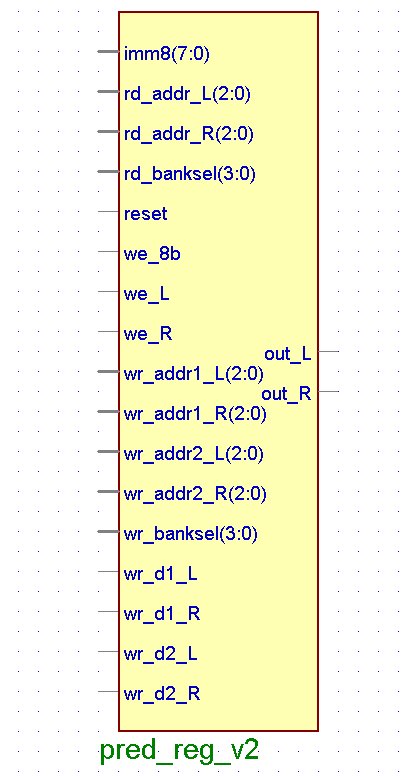
Figure I-2, Predicate register file
PLX has 32 general purpose registers. In our 2-way superscalar, the register file has 4 read ports, 3 write ports (including 1 serves for data from data cache). The implemented register file is included in regfile.vhd.4.1.6 INSTRUCTION DECODER
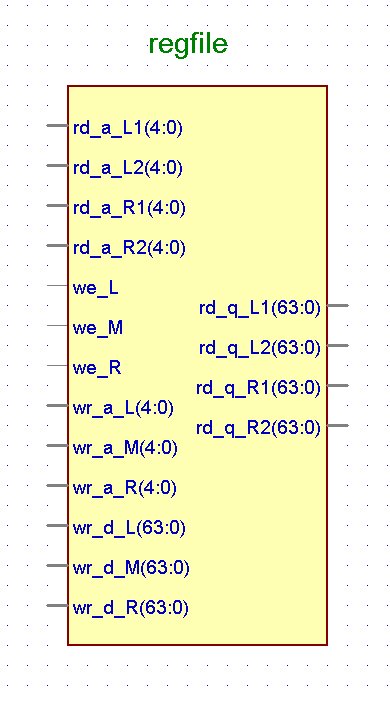
Figure I-3, General purpose register file
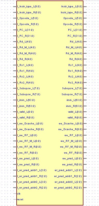
Instruction decoder interprets instructions: it separates predicate register field, Opcode, register fields, immediate number fields and Subop fields, it also sets/clears write-enable bits for different instructions. The coeded instruction decoder is shown in Inst_decoder.vhd.4.1.7 PIPELINE REGISTERS
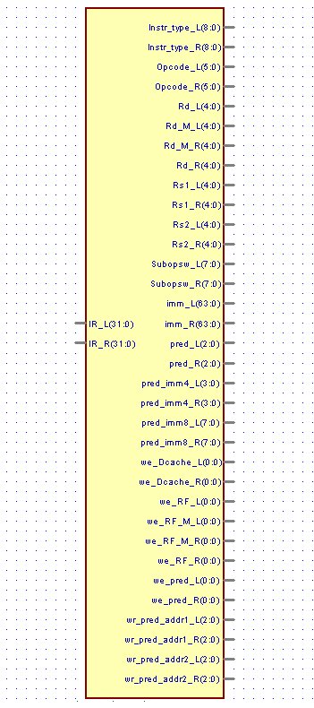
Figure I-4, Instruction decoder
Pipeline registers pipelined all necessary information for all fetched instructions, such as all the decoded fields, the PC and even the instruction itself. An exemplary pipeline register for the control path is included in Ctrl_reg.vhd4.1.8 CONTROLLER

Figure I-5, Pipeline registers
The controller is a pure combinational logic. Indeed, it just checks all kinds of hazards and stalls the pipeline or forwarding correct data. It contains standard data forwarding logic for both general purpose register file and predicate register file. It also deals with WAW hazard elimination. The VHDL code of the controller is in Ctrl_unit.vhd.
The instruction memory, which stores the binary instructions is designed behaviorally as an array of std_logic_array(31:0). Therefore the memory structure is 4 byte Big-Endian words. The memory size is defined as 1Kb, with 1024/4 wordlines. As there is no standard defined for initializing the Imem, we first read the binary file generated by the assembler that contains the binary instructions. As the I-mem is byte addressed, the references should be aligned by 4 bytes. This should be seriously taken into consideration in 'jmp' instructions' offsets. The VHDL code for the instruction memory is shown in I_Cache.vhd.
The data memory, which loads/stores the memory data is designed behaviorally similar to the instruction memory as an array of std_logic_array(31:0). It is also 4 byte word, Big-Endian addressable and size is 1Kb with 1024/4 wordlines. In addition to the Waddr and Raddr address lines, and the Wdata data line, there is a we write enable signal to suppress/enable writes depending on the instruction. The VHDL code for Data cache is in D_Cache.vhd
The top level design is as shown in the following figure, the corresponding VHDL file is in PLX.vhd.4.2) APPENDIX-II - ALU TEST:
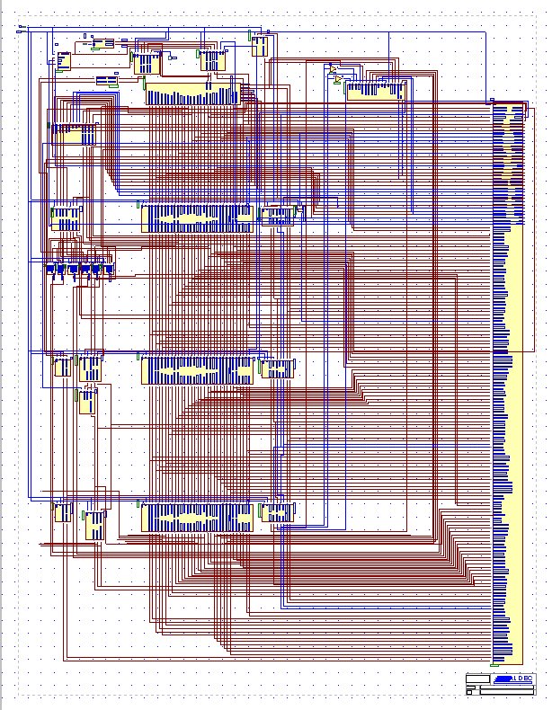
Figure I-6, Top level block diagram
To test the ALU functionality, we wrote a small testbench
for the ALU. The test file performs
one operation within a defined time period and performs the respective
operations:
The ALUout values for Padd operations are obvious. For the compare instructions, we only regard the sign information for >,< relations, therefore, the ALU code reveals only the correct sign information for the operation for the unsigned comparisons. A positive value means the first operand is bigger, while a negative value means the second operand is bigger, in terms of the applied comparison method. The test file is written for a pattern period of 100 ns, so the whole test set is applied in 900 ns. The resultant simulation waveforms are as shown in the following figures AppII-1, and AppII-2.
- Period 1: padd.8 15, 32
Expected ALUout: 47
- Period 2: padd.8 -99, 32
- Period 3: padd.2 x35_24_45_23, x00_00_11_11
- Period 4: cmp.eq 10, -10
- Period 5: cmp.ge -8, 764
- Period 6: cmp.geu -8, 764
- Period 7: cmp.geu 764,-8
- Period 8: cmp.geu -764, -8
- Period 9: cmp.geu 764,8
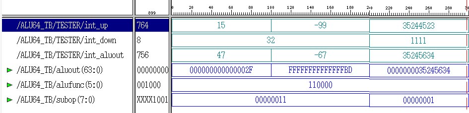
Hence, figure AppII-1 is actually two merged figures, the first 2 patterns are displayed as signed integers, to demonstrate the padd.8 operation and the 3rd period displays the patterns in HEX to simplify the observation of padd.2 operation.
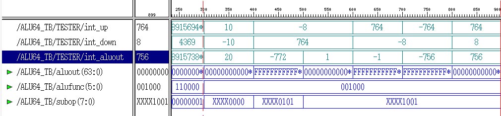
As seen in figure AppII-2, the described compare operations are performed
and the results are in accordance with expectations.
In these test programs, we also use a batch simulation option provided
by the Synopsys Software, named comm
files. These files automate the simulation, by letting the user pre-store
the desired simulator actions. The used comm file for the ALU test is included
in ALU64test2. Information on how to
use these files can be found in the text
file about how to use batch files. As an example, for the ALU test,
after starting the simulator, typing:
enables the use of the comm file and produces the above shown simulation results.# include ./batchfiles/ALU64test2
# ALU64comm2